")
") Deutsch (Germany)
Deutsch (Germany) ") Polski (PL)
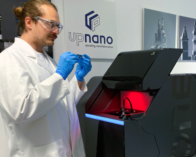
Polski (PL) Production of embedded microfluidic chips as well as tungsten and platinum microstructures with (sub-)micron resolution possible with UpNano's NanoOne printer
Sidebar
Electronics


The Evolution of the Electronics Industry
A Deep Dive into the Growth of PCB, Flexible PCBs, and Sensors
By Afnan Islan, Vice President, BotFactory, Inc.
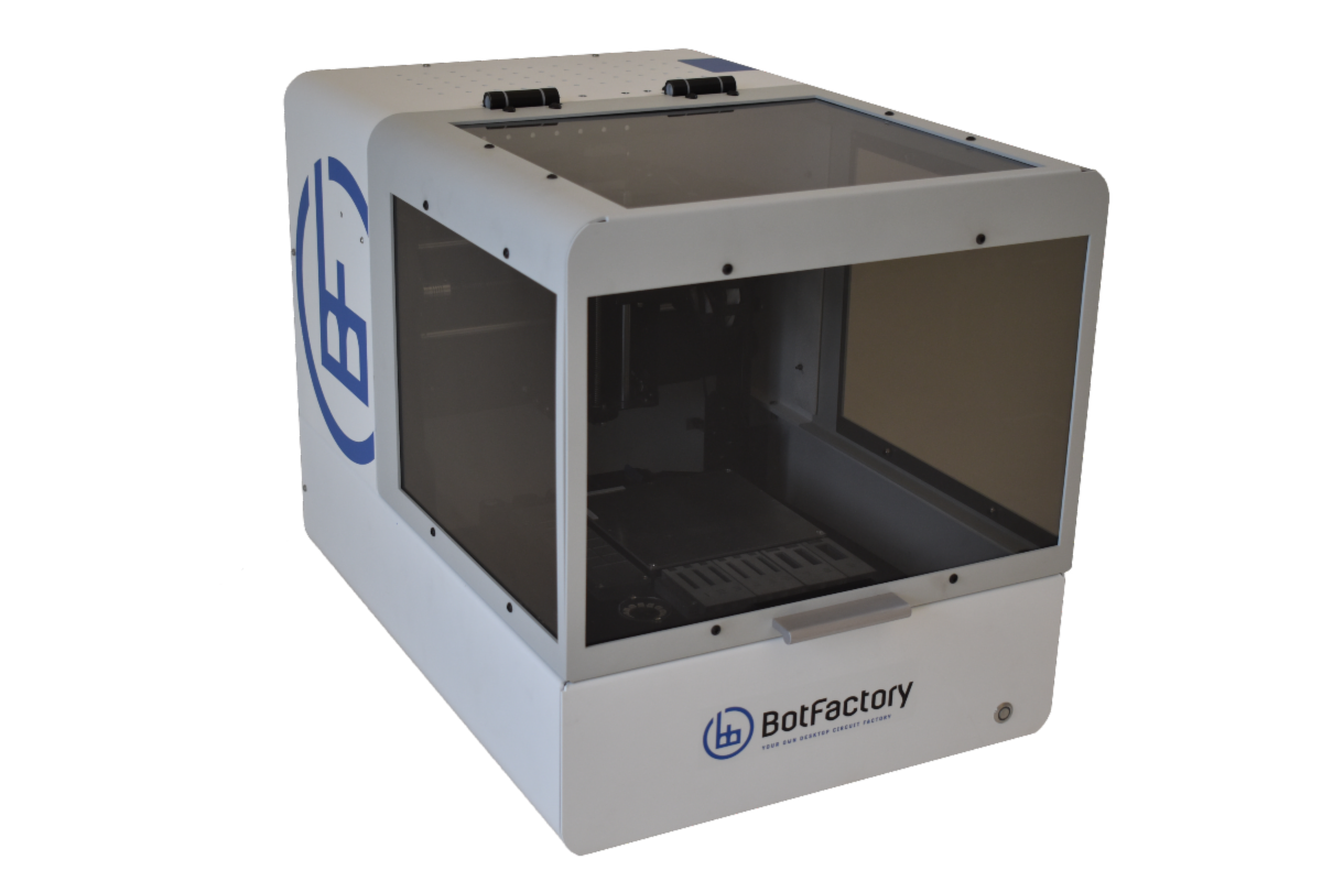
BotFactory Highlights the SV2 All-in-One Desktop
3D PCB Printer and Pick-and-Place Machine
Efficient and cost effective machine allows users to prototype PCBs in minutes instead of weeks

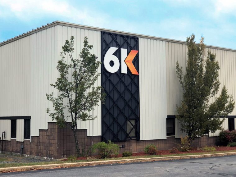
Tennessee Governor Bill Lee Joins 6K Executives for Official Groundbreaking Ceremony for the PlusCAM Battery Material Production Plant in Jackson, TN
The company also announced partnerships with a team of professional design and construction contractors Ghafari, Evans General Contractors, Koch Project Solutions for plant construction.
Additive Manufacturing sparks innovation
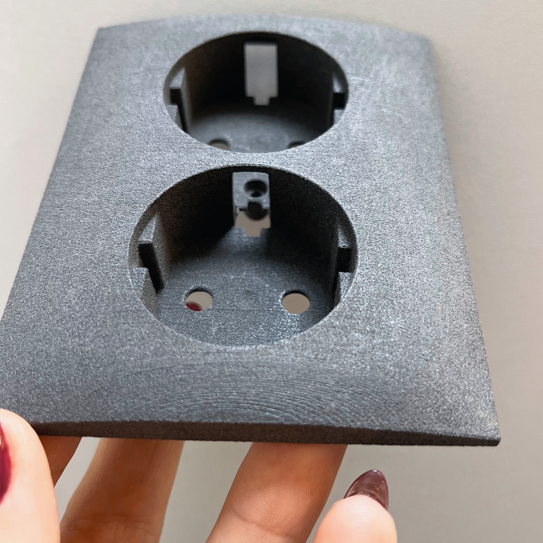
Polish company Kontakt-Simon SA uses the Sintratec S2 to build advanced prototypes for the electrical sector. Thanks to the Selective Laser Sintering technology, the R&D team can rapidly develop and verify their complex designs.
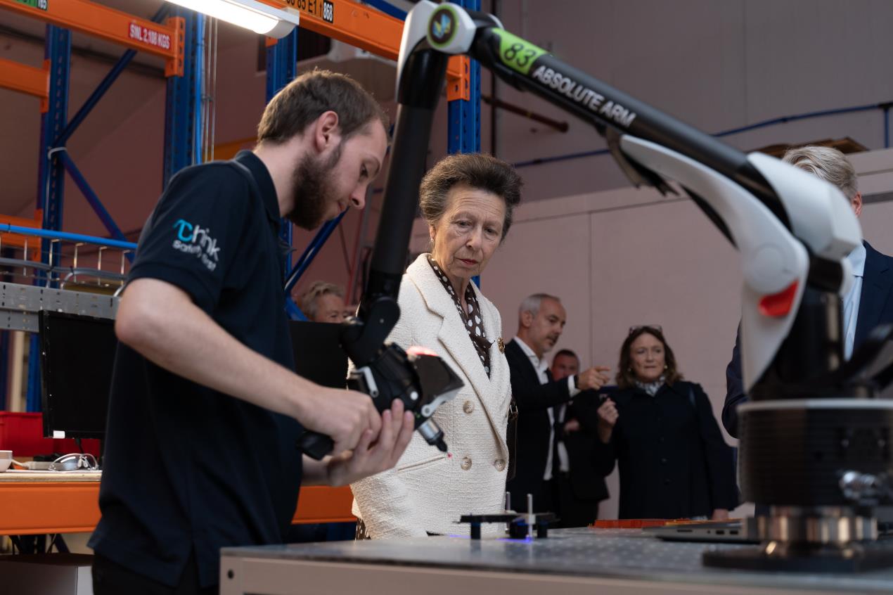
HRH The Princess Royal visits Photocentric
Photocentric, inventor of LCD 3D printing, welcomed Her Royal Highness, The Princess Royal to its Peterborough headquarters at Cambridge House, Oxney Road, Peterborough.
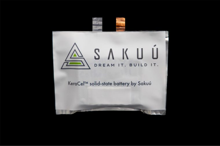
Sakuú Corporation Develops 3Ah Lithium Metal Solid-state Battery that Offers Improved Energy Performance over Market’s Existing Options
New and safe 3Ah lithium-metal, 30 sub-cell, solid-state battery could deliver even greater energy performance than current lithium-ion batteries by up to 25% in future.
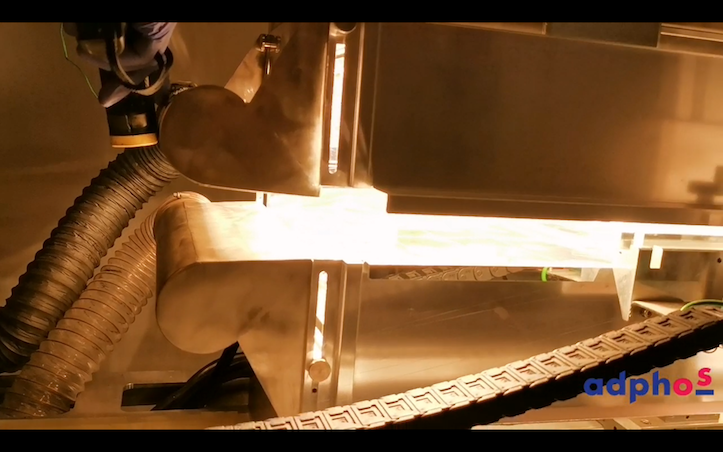
adphos aLITE – processing integrated in multilayer 3D-battery and energy storage production
Complex multilayer production process consisting of electronical and insulation conduction layers, anode/cathode layers, sealings and electrolyte paste based layers, either solvent or water-based, with wet coating thicknesses between a few microns (≤ 15 µm) up to several hundred (even ≥ 500 µm) are dried and sintered with coatings/layers adapted aLITE® process steps, all within one-digit seconds (even partially ≤ 1 s).
Sakuu Poised to Unlock Mainstream Adoption of Electric Vehicles with World’s First EV Battery 3D Printer
New multi-material, multi-process additive manufacturing platform solves issues of performance and cost, using 50% fewer materials to deliver up to twice the energy capacity in the same space or the same energy in half the space
6K Prepares for Major Advancement in Battery Materials with $25M Investment
Battery Center of Excellence will provide a gateway to bring production of batteries to the United States and answer the call to President Biden’s Executive Order to create a more resilient and secure supply chain
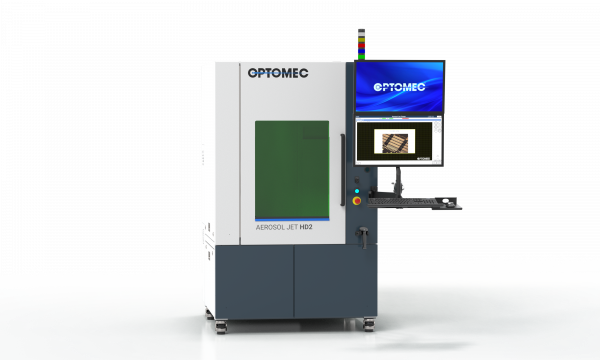
Optomec Introduces New 3D Additive Electronics Printer for Inline Production
The Aerosol Jet HD2 is optimized for Advanced Semiconductor Packaging including mmWave applications
Latest Sponsor News
Articles Most Read


Latest News


Statistics
- Articles View Hits
- 3877132
Who's Online
We have 75 guests and no members online